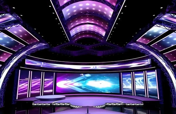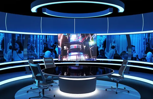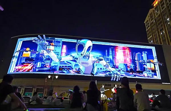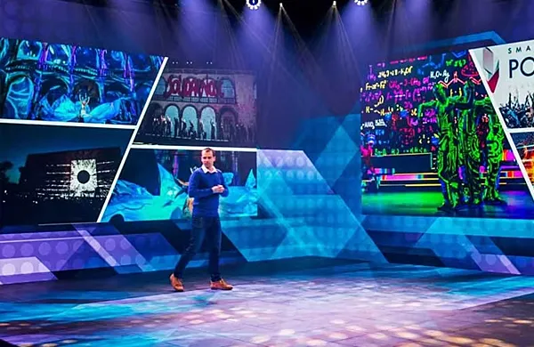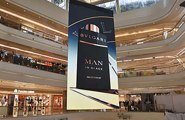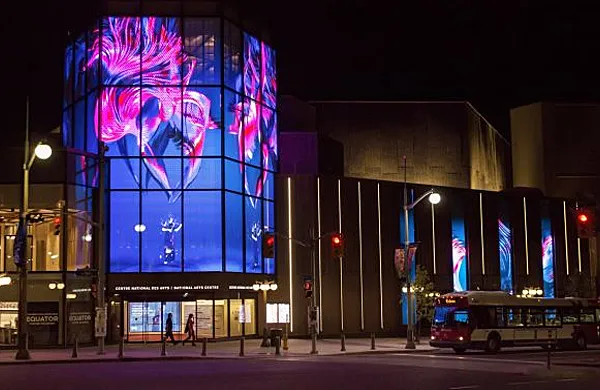

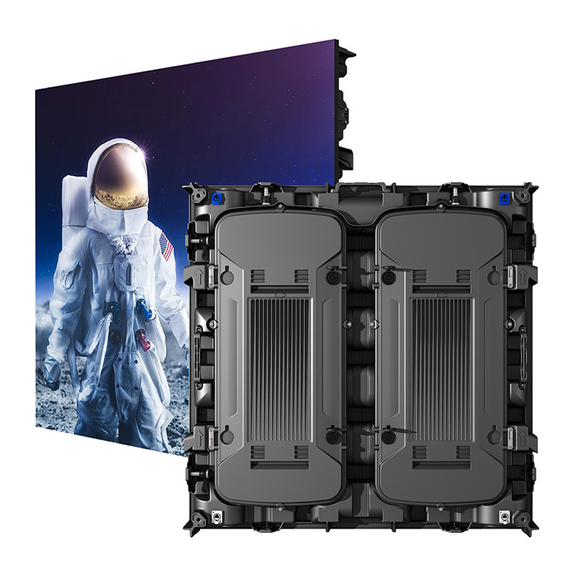
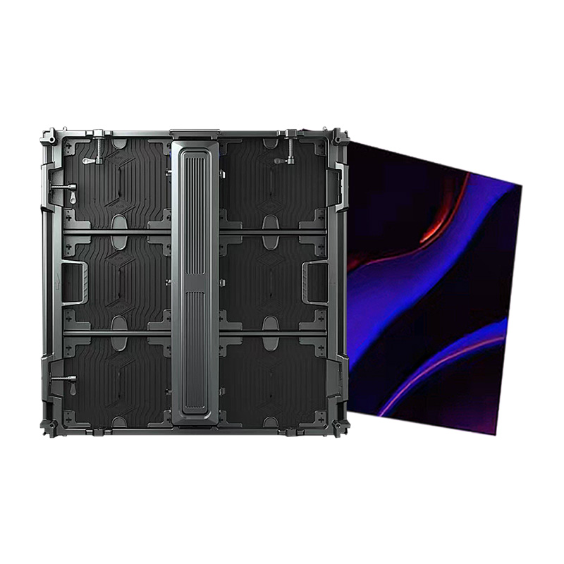
ModernsLED displeju ekrānipaļaujas uz pusvadītāju elektroluminiscenci, kur InGaN/GaN mikroshēmas izstaro zilu gaismu (450 nm), kas ar fosfora pārklājuma palīdzību tiek pārveidota baltā krāsā. Augstas klases displeji sasniedz 16 bitu pelēktoņus, 3840 Hz atsvaidzes intensitāti un 5000 nitu spilgtumu lietošanai ārpus telpām.
TipsInGaN zilās mikroshēmas (2835/1010 iepakojumi)
Specifikācijas:
Viļņa garums: 450 ± 2 nm
Priekšējais spriegums: 2,8–3,4 V @ 20 mA
Gaismas efektivitāte: ≥180 lm/W
| Materiāls | Īpašumi | Pieteikums |
|---|---|---|
| Epoksīda sveķi | Refrakcijas indekss 1,53, ΔYI <2 | LED LAMPAS |
| Silikons | Caurlaidība 95%, CTE 250 ppm | SMD/mini gaismas diodes |
| Elektromagnētiskā saderība | Bez halogēna, TG 150 ℃ | Automobiļu displeji |
Alumīnija PCBSiltumvadītspēja ≥2,2 W/m·K, Cu biezums 35±5 μm
Keramikas PCBAlN substrāti (24 W/m·K) lieljaudas LED masīviem
LīmeSudraba epoksīdsveķi (80% Ag saturs)
Konservēšana150 ℃/1 h, savienojuma līnijas biezums 25 ± 5 μm
PrecizitāteNovietošanas kļūda ≤±15μm
Vads99,99% Au, diametrs 1,0 mili
ParametriUltraskaņas jauda 50 W, spēks 30 g, cikla laiks 0,3 s
ProcessVakuuma iepildīšana (≤1kPa, 30 minūšu degazācija)
Konservēšana135 ℃/4 stundas, burbuļa diametrs ≤30 μm
Tapu veidošanaBīdes griešana ±0,1 mm pielaide
BinningViļņa garums ±2 nm, gaismas intensitāte ±5%
TrafaretsLāzergriezts nerūsējošais tērauds, 0,12 mm biezums
LodētSAC305 sakausējums, tilpums 80–120 μm (SPI monitorings)
MašīnaĀtrgaitas paņemšana un novietošana (30 000 apgriezieni stundā)
Precizitāte: ±0,03 mm (X/Y), ±0,5° (θ)
Profils:
Uzkarsēšana: 1-2 ℃/s līdz 150 ℃
Maksimālā temperatūra: 245 ℃ (60 s virs 217 ℃)
AtmosfēraSlāpeklis (O₂ <1000 ppm)
FormēšanaPārneses process @8-12MPa, 150℃/180s
Lāzergriešana355 nm UV lāzers, 5 W jauda, 100 mm/s ātrums
Lāzera pacelšanās (LLO):
Pārneses ātrums: 99,99% (pētniecība un attīstība), 99,9% (ražošana)
Precizitāte: ±1,5 μm izvietojums
Pikseļu blīvums100–200 pikseļi collā
IekapsulēšanaMelns epoksīda pildījums (ΔE <1,5)
AEC-Q102Darbības temperatūra: no -40 ℃ līdz 125 ℃, 85 ℃/85 % relatīvais mitrums/1000 h
Vibrācijas tests50G triecienizturība (MIL-STD-883 metode 2002)
AOIDefektu noteikšana ≥99,9% (lodēšanas tiltiņi, trūkstošas detaļas)
RentgensLodēto savienojumu tukšums <15%
| Tests | Nosacījumi | Prasības |
|---|---|---|
| Termiskā riteņbraukšana | -40 ℃ ↔85 ℃, 1000 cikli | Gaismas plūsmas noturība ≥97% |
| Sāls aerosols | 5% NaCl, 96 stundas | Korozijas laukums ≤3% |
| IR | 130℃/85% relatīvais mitrums, 96 stundas | UN ≥100 MΩ |
Integrējošā sfēraCCT pielaide ±150K, CRI ≥80
Skata leņķis≥140° horizontāli/vertikāli, ≤50% spilgtuma kritums
MSL līmenis3. līmenis (72 stundu grīdas kalpošanas laiks @ 30℃/60% relatīvais mitrums)
Sausais iepakojums<10% relatīvais mitrums ar desikantu
ISTA 3AIztur 1,2 miljonu kritienu, 50G triecienus
DrošībaUL/cUL, CE, CCC sertifikāts
VidesRoHS 2.0, REACH SVHC <0,1 %
Karsti ieteikumi
Karstie produkti
Saņemiet bezmaksas cenu piedāvājumu tūlīt!
Sazinieties ar mūsu pārdošanas komandu tūlīt.
Ja jūs interesē mūsu produkti, lūdzu, sazinieties ar mums nekavējoties
Sazinieties ar mūsu pārdošanas komandu, lai izpētītu pielāgotus risinājumus, kas lieliski atbilst jūsu uzņēmuma vajadzībām, un atbildētu uz visiem jūsu jautājumiem.
E-pasta adrese:info@reissopto.comRūpnīcas adrese:6. ēka, Huike plakanā paneļa displeju industriālais parks, Nr. 1, Gongye 2. ceļš, Shiyan Shilong kopiena, Bao'an rajons, Shenzhen pilsēta, Ķīna
WhatsApp:+8615217757270